Voltage Regulator Calculator
This calculator was created to give the designer the optimum values for voltage regulator set resistors, given a value for the reference voltage. See the description below the calculator for more information.

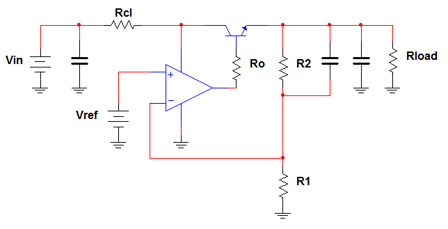
The voltage regulator circuit shown above is a special case of the non-inverterting op amp topology. In this application, it is optimized for DC response. Some - or most of the components may be inside the IC. A switching supply may add an inductor and second transistor. I'll go through the general circuit components and their impact on circuit operation in more detail below:
- The input voltage. Care should be taken that the input voltage not exceed the ratings of the op amp - or regulator IC. It is possible in the case of some IC's, especially switching IC's, to operate the active portions of the circuit on a lower voltage than the transistor / switching elements that form the power pathway.
- Input voltage decoupling. This usually consists of low frequency electrolytic and high frequency ceramic elements. Component selection may be critical for switching power supply stability.
- A current limiting resistor. This can be a safety component to limit the amount of current that will flow in a short circuit condition, but it is a bit of a balancing act. The op amp voltage swing may start rising to the point that it can no longer compensate its loop as the load current rises.
- The transistor - called a pass transistor. It can be either an NPN bipolar, or an N-CH FET. The circuit will operate almost the same way. In the case of an FET, however, gate capacitance can make the op amp unstable. A small series resistance will solve that problem, and may even be a good idea to limit base current to a bipolar transistor.
- The voltage reference may be supplied externally in some cases, or fabricated on the IC. If an external reference is used, it can be powered off of the input voltage, or off of the supply that drives the op amp. The important thing is that it be low noise and stable under all conceivable operating conditions.
- The op amp performs the function of balancing the output from the emitter or source of the pass transistor with the reference voltage. The action of the op amp, after all, is to drive its output to whatever voltage is required to make its inverting and non-inverting inputs the same voltage. Because the op amp output is connected to the base or gate of the pass transistor, it usually will rise a few tenths of a volt over the output voltage. The inverting input of the op amp is connected to a scaled version of the output voltage through a voltage divider comprised of R1 and R2 - which are set to match the reference voltage when the output voltage is the right value. A capacitor across the top resistor is effective in lower the operating frequency of the op amp, effectively forming a low pass filter. Some regulators recommend a capacitor across the bottom resistor - for reasons related to how their internal circuitry is implemented.
- The output of the regulator circuit needs to be decoupled. In the case of switching supplies, this is critical to the amount of ripple voltage that can be tolerated in the application, and maybe to the stability as well.

